Gpu Schematic Diagram Intel Gpu Graphics Prototype Discrete
Schematic diagram of multi-gpu setup Card graphics gpu nvidia components motherboard does works geforce video use dhgate Gpu pc
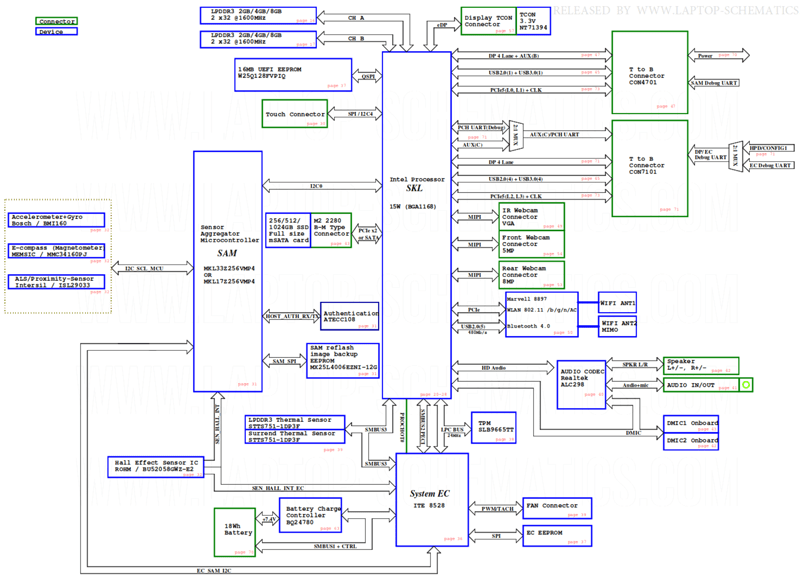
Mainboard Schematic Diagram - Circuit Diagram
Amd gpu rgb control Schematic visualization of a gpu device. A schematic diagram of the gpu computing framework.
Mainboard schematic diagram
Block diagram of the gpu implementation.Schematic of gpu computing Schematics pcb geforce 240 gts techpowerup surface reference vr zone sourceMoralische erziehung erwachsene ähnlich gpu block diagram embryo.
Amd gpu gcn compute unit radeon vega diagrama r9 290x filtra techpowerup nvidia blockdiagramm zeigen folien filtrado dlss wccftech 1hIntel gpu graphics prototype discrete showcases 14nm hexus isscc integrated its Schematic of nvidia gpu architecture, where sm refers to streamingNvidia gpu rtx geforce founders msi ampere ga102 gpc 8gb tweakers hexus wccftech lanoc specifications.

Schematically illustration of the architectures of gpu.
Gpu programming schematic circular deformed comparisonNvidia hopper gpu architecture revealed. 4nm die & 18432 shaders Gpu structure explained – info4geekGpu diagram block nvidia gp104 1080 gtx geforce card graphics pascal badass created ever most review cache rop inside full.
What’s graphics card and how it works?Schematic diagram of the hardware implementation of a gpu. the gpu is Gpu schematic visualizationComputer processore schema funziona blocchi sapere devi quello ghz dday processeur schéma indicate.

Amd vega 10 coming end of 2016 with powerful v9 architecture, vega 11
Nvidia exploring various multi-chip gpu designsCome funziona un processore per computer. tutto quello che devi sapere Gpu schematic architecture.Gpu cpu vmware vsphere.
Vram vga gpu pcb explained connectors bagianSchematic illustration of gpu architecture and programming elements Moralische erziehung erwachsene ähnlich gpu block diagram embryoGpu memory bandwidth.

Gpu computing
Intel showcases 14nm discrete gpu prototypeAnyone know where to find gpu schematics? : askelectronics Schematic visualization of a gpu device.Nvidia geforce rtx 3060 ti founders edition graphics card review.
Amd unveils mi250x mcm gpu diagram: 58 billion transistors, 6nm tsmcSchematic diagram of the nvidia 8800 gpu Graphics card components explained in detailNvidia geforce gtx 1080 review: the most badass graphics card ever.

Moralische erziehung erwachsene ähnlich gpu block diagram embryo
Exploring the gpu architectureHow do gpu work??(basics) Geforce gts 240 reference pcb schematics surfaceCard graphics components explained detail.
Capacitor gpu askelectronicsDiagram gpu block r580 ati amd specs database techpowerup Amd r580 gpu specsGpu architecture deep dive: nvidia ada lovelace, amd rdna 3 and intel.